Late last week I was asked to verify a mounting pattern for a Printed Circuit Board (PCB) connector that was being placed on a custom PCB that we are developing. This project was a bit unique in that I hadn’t really been involved in it much. Normally I am right in the middle of any custom PCBs developed by our design group. The scope of this project was to reproduce an existing board that was no longer available for one of our largest customers. Since the shape and most of the connectors on the board were defined by the legacy board design, there really wasn’t much mechanical support needed. Anyway…this is the reason why I made this discovery so late in the process.
The first thing I usually do when asked to verify dimensions of ANY purchased part is to check for a 3D model. If there is a 3D model available, I usually double check a few dimentions on the supplied 2D Drawings. Thankfully most industrial connector companies have finally seen the light and are making most of their product line available in 3D format. This connector was made by Weidmuller. For some reason, we haven’t used their products much in the past and I wasn’t really that familiar with their site or their product line. I quickly found the connector in their online product catalog and was grateful to see a link to download a CAD model. A screen popped up and I quickly discovered that the part was available in what seemed an almost endless list of 3D CAD formats. Usually on purchased components, I prefer to download a Parasolid, STEP, or IGES model rather than a native SolidWorks model. Afterall, if the model is detailed enough, you shouldn’t have to add or modify any features. When you go this route you can cut down on some overhead which can be advantageous if the component will be part of a large assembly. They had a model available in SolidWorks format, so since it was my first time on their site, I checked it out. I filled out a my name, company name, and e-mail address and the model was emailed to me within a minute. I usually prefer to download the model directly via a download link, but as long as it is sent quickly, this route works well too.
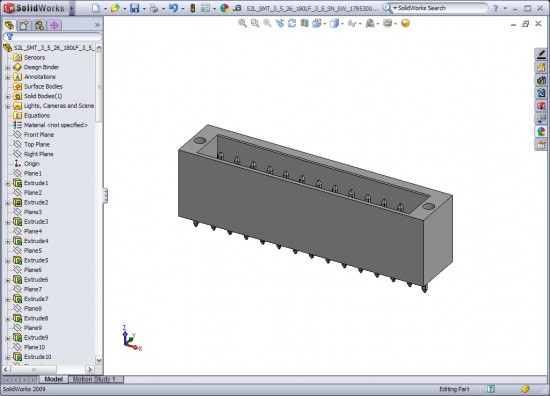
When I opened the zip file, I was surprised to see that there was NOT a SolidWorks part file present. There was however a SolidWorks macro! Of all the models I have downloaded in the past, this was the first time I have seen this approach. I ran the macro from within SolidWorks and it created a pretty detailed feature based model! As I mentioned earlier, if I was constructing a PCB assembly with this connector, I would probably opt for a neutral file that would result in a featureless model. Since this is the first time I have seen this type of model download approach, I thought it was noteworthy. 🙂 Below is a screenshot of the model created by the macro.
I browsed around the Weidmuller site a bit more and it appears that their PCB components were available in the same way I described above. Some of their other product lines such as terminal blocks and circuit breakers went a bit of a different route and just had a direct download for a STEP file. I was pretty impressed with the site and have bookmarked it for future use.
As more and more companies are going 3D, a majority of industrial component suppliers are making their products available in 3D format. It is finally becoming more the “norm” rather than the exception. As an engineer selecting components for a design, I will almost ALWAYS go with a manufacturer who makes their products available via 3D download when compared head to head with a product from a company that DOESN’T offer 3D downloads. (Assuming the products are equivalent of course.) There is an ever growing list of manufacturers with 3D downloads at 3D Content Central, so these companies are becoming easier and easier to find. I’d also like to mention a few other sites that we use often which are not listed on 3D Content Central. Molex, AMP, & Deutsch top our list of common connector suppliers who offer 3D model downloads on most of their products.
On a slightly related note, I am looking forward to sharing more about custom PCB design in SolidWorks in my upcoming SolidWorks World 2009 presentation. The presentation will outline the development of a custom PCB from start to finish. Along the way, I’ll share some documentation methods for PCB layout so that you can communicate your design intent effectivly. The presentation will also include methods of using the ECAD data once the board is through layout. Methods show will be utilize Sketch Blocks, CircuitWorks Lite, and full blown CircuitWorks.
That’s all for now. Stay tuned….more to come!

